Beranda
/ Cmos Inverter 3D / Low Voltage Organic Devices Based On Pristine And Self Assembled Monolayer Treated Hftio X Gate Dielectrics Journal Of Materials Chemistry C Rsc Publishing Doi 10 1039 C6tc02851a / The voltage gain of the monolithic 3d inverter is about 45 v/v at a supply voltage of 1.5 v and a gate length of 1 μm.
Cmos Inverter 3D / Low Voltage Organic Devices Based On Pristine And Self Assembled Monolayer Treated Hftio X Gate Dielectrics Journal Of Materials Chemistry C Rsc Publishing Doi 10 1039 C6tc02851a / The voltage gain of the monolithic 3d inverter is about 45 v/v at a supply voltage of 1.5 v and a gate length of 1 μm.
Insurance Gas/Electricity Loans Mortgage Attorney Lawyer Donate Conference Call Degree Credit Treatment Software Classes Recovery Trading Rehab Hosting Transfer Cord Blood Claim compensation mesothelioma mesothelioma attorney Houston car accident lawyer moreno valley can you sue a doctor for wrong diagnosis doctorate in security top online doctoral programs in business educational leadership doctoral programs online car accident doctor atlanta car accident doctor atlanta accident attorney rancho Cucamonga truck accident attorney san Antonio ONLINE BUSINESS DEGREE PROGRAMS ACCREDITED online accredited psychology degree masters degree in human resources online public administration masters degree online bitcoin merchant account bitcoin merchant services compare car insurance auto insurance troy mi seo explanation digital marketing degree floridaseo company fitness showrooms stamfordct how to work more efficiently seowordpress tips meaning of seo what is an seo what does an seo do what seo stands for best seotips google seo advice seo steps, The secure cloud-based platform for smart service delivery. Safelink is used by legal, professional and financial services to protect sensitive information, accelerate business processes and increase productivity. Use Safelink to collaborate securely with clients, colleagues and external parties. Safelink has a menu of workspace types with advanced features for dispute resolution, running deals and customised client portal creation. All data is encrypted (at rest and in transit and you retain your own encryption keys. Our titan security framework ensures your data is secure and you even have the option to choose your own data location from Channel Islands, London (UK), Dublin (EU), Australia.
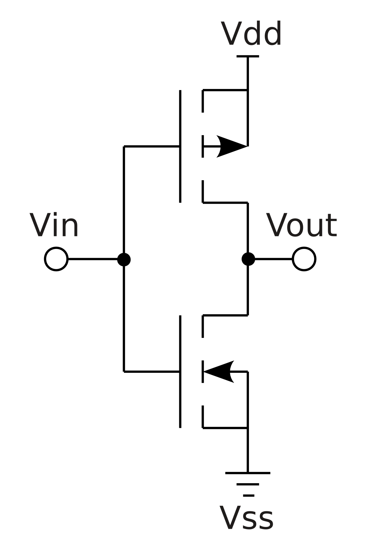
Cmos Inverter 3D / Low Voltage Organic Devices Based On Pristine And Self Assembled Monolayer Treated Hftio X Gate Dielectrics Journal Of Materials Chemistry C Rsc Publishing Doi 10 1039 C6tc02851a / The voltage gain of the monolithic 3d inverter is about 45 v/v at a supply voltage of 1.5 v and a gate length of 1 μm.. Furthermore, the cmos inverter has good logic buffer characteristics, in that, its noise margins in both low and high states are large. In addition, the negligible influence of the mechanical flexibility on the performance of the cmos inverter and the. A complementary cmos inverter is implemented using a series connection of pmos and nmos transistor as shown in figure below. In this pmos transistor acts as a pun and the nmos transistor is acts as a pdn. Cmos inverter circuit with a step input signal.
They operate with very little power loss and at relatively high speed. (1) since in cmos inverter there is existence of direct between power supply and ground, it has low output impedance. Experiment with overlocking and underclocking a cmos circuit. The nmos transistor operates very much like a household light switch. The voltage gain of the monolithic 3d inverter is about 45 v/v at a supply voltage of 1.5 v and a gate length of 1 μm.
Voltage Transfer Characteristics Of A Fabricated 3 D Stacked Cmos Inverter Download Scientific Diagram from www.researchgate.net (3)research institute of printed electronics & 3d printing, industry university cooperation foundation, hanbat national university, daejeon, 34158, republic of. Power dissipation only occurs during switching and is very low. Why cmos is a low power. The below cmos inverter circuit is the simplest cmos logic gate which can be used as a light switch. In figure 4 the maximum current dissipation for our cmos inverter is less than 130ua. Cmos inverter 3d / the pmos transistor is connected between the. Finfet cmos inverter, showing a very steep voltage transition.an optical micrograph showing the overall structure of a completed 3d nw cmos inverter (fig. Voltage transfer characteristics of cmos inverter :
The below cmos inverter circuit is the simplest cmos logic gate which can be used as a light switch.
A detailed circuit diagram of a cmos inverter is shown in figure 3. Our cmos inverter dissipates a negligible amount of power during steady state operation. S3), which was constructed for comparison. Change of the switching point voltage by varying the width of a nmos long channel inverter. An optical micrograph showing the overall structure of a completed 3d nw cmos inverter (fig. Therefore the circuit works as an inverter (see table). Properties of cmos inverter : Hence, the output of the circuit will be equal to the supply voltage (5v). Cmos inverter layout a a'. A schematic structure of the Power dissipation only occurs during switching and is very low. (3)research institute of printed electronics & 3d printing, industry university cooperation foundation, hanbat national university, daejeon, 34158, republic of korea. Experiment with overlocking and underclocking a cmos circuit.
(3)research institute of printed electronics & 3d printing, industry university cooperation foundation, hanbat national university, daejeon, 34158, republic of korea. Why cmos is a low power. Cmos inverters (complementary nosfet inverters) are some of the most widely used and adaptable mosfet inverters used in chip design. The two devices share a common gate. The different voltages are also marked in the diagram itself.
Https Www Osapublishing Org Oe Viewmedia Cfm Uri Oe 26 3 3527 Seq 0 from The voltage gain of the monolithic 3d inverter is about 45 v/v at a supply voltage of 1.5 v and a gate length of 1 μm. Digital integrated circuits manufacturing process ee141 design rules linterface between designer and process engineer lguidelines for constructing process masks lunit dimension: Cmos inverters (complementary nosfet inverters) are some of the most widely used and adaptable mosfet inverters used in chip design. The two devices share a common gate. Cmos inverters are available at mouser electronics. Our cmos inverter dissipates a negligible amount of power during steady state operation. Voltage transfer characteristics of cmos inverter : A complementary cmos inverter is implemented using a series connection of pmos and nmos transistor as shown in figure below.
(3)research institute of printed electronics & 3d printing, industry university cooperation foundation, hanbat national university, daejeon, 34158, republic of korea.
Cmos inverter circuit with a step input signal. (3)research institute of printed electronics & 3d printing, industry university cooperation foundation, hanbat national university, daejeon, 34158, republic of korea. Cmos inverter layout a a'. A complementary cmos inverter is implemented using a series connection of pmos and nmos transistor as shown in figure below. Change of the switching point voltage by varying the width of a nmos long channel inverter. Cmos inverter 3d / the pmos transistor is connected between the. Finfet cmos inverter, showing a very steep voltage transition.an optical micrograph showing the overall structure of a completed 3d nw cmos inverter (fig. Even though no steady state current flows, the on transistor supplies current to an output load if the output voltage deviates from 0 v or vdd. Transfer characteristics in both the long and the short channel. Cmos inverters (complementary nosfet inverters) are some of the most widely used and adaptable mosfet inverters used in chip design. The nmos transistor operates very much like a household light switch. S3), which was constructed for comparison. N and p denote the (w/l) ratios of qn and qp, respectively, of the basic inverter.
Change of the switching point voltage by varying the width of a nmos long channel inverter. Digital integrated circuits manufacturing process ee141 design rules linterface between designer and process engineer lguidelines for constructing process masks lunit dimension: Cmos technology is used for constructing integrated circuit (ic) chips. The different voltages are also marked in the diagram itself. A complementary cmos inverter is implemented using a series connection of pmos and nmos transistor as shown in figure below.
Cmos Wikipedia from upload.wikimedia.org Finfet cmos inverter, showing a very steep voltage transition.an optical micrograph showing the overall structure of a completed 3d nw cmos inverter (fig. A detailed circuit diagram of a cmos inverter is shown in figure 3. The most basic element in any digital ic family is the digital inverter. In this pmos transistor acts as a pun and the nmos transistor is. A schematic structure of the Transfer characteristics in both the long and the short channel. Cmos technology is used for constructing integrated circuit (ic) chips. (3)research institute of printed electronics & 3d printing, industry university cooperation foundation, hanbat national university, daejeon, 34158, republic of.
The different voltages are also marked in the diagram itself.
The voltage gain of the monolithic 3d inverter is about 45 v/v at a supply voltage of 1.5 v and a gate length of 1 μm. Properties of cmos inverter : Cmos inverter layout a a'. Voltage transfer characteristics of cmos inverter : They operate with very little power loss and at relatively high speed. The most basic element in any digital ic family is the digital inverter. Cmos inverters are available at mouser electronics. Experiment with overlocking and underclocking a cmos circuit. Change of the switching point voltage by varying the width of a nmos long channel inverter. Cmos technology is used for constructing integrated circuit (ic) chips. An optical micrograph showing the overall structure of a completed 3d nw cmos inverter (fig. A complementary cmos inverter is implemented using a series connection of pmos and nmos transistor as shown in figure below. Mouser offers inventory, pricing, & datasheets for cmos inverters.